Strained Silicon On Insulator Wafers

Strained Silicon On Insulator
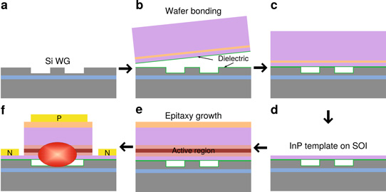
Indium Phosphide Template For Laser And Silicon On Insulator Integration

Breakthrough In Silicon Technology Wafer Level Strained Silicon Technology Announced By Sigen

Stretching Silicon S Lifespan Sciencedirect

Pdf Fabrication Of Silicon On Insulator Soi And Strain Silicon On Insulator Ssoi Wafers Using Ion Implantation

Products Soitec Soitec
This gives rise to a highly nonequilibrium laser process and can vary significantly to that in normal bulk silicon substrate.
Strained silicon on insulator wafers.

Process Flow Of Fabricating Strained Silicon On Bpsg A Handle Wafer Download Scientific Diagram

Strained Silicon On Insulator Ssoi By Waferbonding Sciencedirect

Figure 1 From Impact Of Strained Silicon On Insulator Ssoi Substrate On Finfet Mobility Semantic Scholar

Strained Silicon On Soi Substrates Adds Up Ee Times

Strained Silicon An Overview Sciencedirect Topics
Http Link Springer Com Content Pdf 10 1007 2fs11664 003 0232 X Pdf

Materials And Manufacturing Techniques For Silicon On Insulator Soi Wafer Technology Sciencedirect

Global Strain

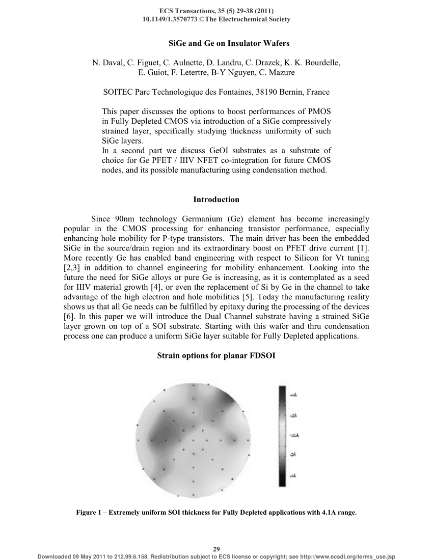
Color Online A 21 Points Strain Map Obtained From A 300 Mm Strained Download Scientific Diagram
Http Www Qdgroup U Psud Fr Publications Sse2004 Pdf
Design Trade Considerations For Blended Wing Body Vs Standard Cylindrical Fuselage Designs

Strain Engineering In Functional Materials Aip Advances Vol 9 No 3

Strain Evolution Of Sige On Insulator Obtained By The Ge Condensation Technique Apl Materials Vol 7 No 4

Si Device Layer And Buried Oxide Layer Thickness For Various Types Of Download Scientific Diagram

Knowledge Is Structured In Consciousness
Https Aip Scitation Org Doi Pdf 10 1063 1 5050829

Thick Film Silicon On Insulator Wafers Preparation And Properties Sciencedirect

Silicon On Insulator An Overview Sciencedirect Topics
Http Soiconsortium Eu Wp Content Uploads 2017 08 Fdsoi Technology Overview By Nguyen Nanjing Sept 22 2017 Final Pdf
Https Ieeexplore Ieee Org Iel7 9110268 9117802 09117967 Pdf
Https Ieeexplore Ieee Org Iel7 16 8694031 08675993 Pdf

Pdf Excellent Silicon Thickness Uniformity On Ultra Thin Soi For Controlling Vt Variation Of Fdsoi

Strain Dependence Of Indirect Band Gap For Strained Silicon On Insulator Wafers Applied Physics Letters Vol 93 No 10

A Process Flow For Pmos With Classical Si S D And Pmos With Esige Download Scientific Diagram

Pdf Strained Silicon Devices

Silicon On Insulator An Overview Sciencedirect Topics
A Review Paper On Cmos Soi And Finfet Technology

Next Generation Integrated Circuits 300 Mm Wafers Copper Metallization Low K Dielectric Under Interconnect Lines High K Dielectric Under Gate Silicon On Insulator Ppt Download
Https Scholar Princeton Edu Sites Default Files Sturm Files Jp 140 Pdf

Silicon On Insulator Technology Materials To Vlsi J P Colinge 9781402077739

A Sample Processing Direct Hydrophobic Twisted Bonding Of A Soi Download Scientific Diagram
Pdf Strained Silicon Mosfet Technology

Breaking The Absorption Limit Of Si Toward Swir Wavelength Range Via Strain Engineering Science Advances
Http Soiconsortium Eu Wp Content Uploads 2017 08 Fdsoi Technology Overview By Nguyen Sept 25 2017 Shanghai Final Pdf

Value Added Wafers Push Chips Ahead Aaron Hand Managing Editor 11 1 2002 Semiconductor International At A Glance Although Silicon On Insulator Soi Technology Has Been In The Works For Many Years Leading Chipmakers Are Finally Embracing It For

Pdf Two Dimensional Micro Raman Mapping Of Stress And Strain Distributions In Strained Silicon Waveguides

X Rays Reveal Si Thin Film Defects Compamed Trade Fair

Pdf Frontiers Of Silicon On Insulator
Resonant Raman Spectra Of A The 10 Nm Silicon On Insulator And B Download Scientific Diagram

Soitec Bernin Ii 300mm Soi Silicon On Insulator Semiconductor Technology

Sub 100nm Nmos Vt Lg Roll Off Red Sc Ssoi Black Soi Controls Blue Download Scientific Diagram
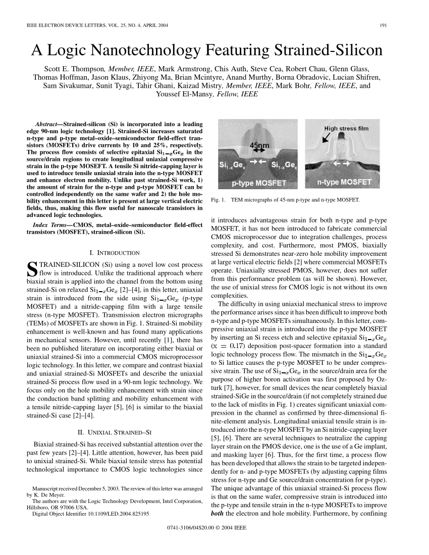
Pdf A Logic Nanotechnology Featuring Strained Silicon
Osa Resonant Cavity Enhanced Responsivity In Germanium On Insulator Photodetectors
Measured Sige Strain In Dual Channel Structures With Soi As Starting Download Scientific Diagram
Source : pinterest.com
